Project Overview
Objective
After designing several simpler PCBs—such as specific power converters or brushless controllers for my drone—I decided to tackle a more challenging design: a board with an integrated microcontroller. An MCU brings new constraints, especially at routing time where many pins and critical signals must be handled. My goal was to stress-test my electronic design skills in a realistic scenario.
Key Features
This board integrates the essentials so the ESP32-S3-MINI-1-N8 can operate reliably: 5V-to-3.3V regulation from USB-C power, a USB-to-UART bridge (FT231XQ-R) for programming and comms, RESET/BOOT tactile buttons, expansion headers for peripherals, status LEDs, and recommended protections/passives to ensure signal integrity and robustness.
Results
A compact, clean and fully functional PCB ready for fabrication. I reinforced skills in custom library creation (symbols & footprints), complete schematic capture, rules/constraints management, multilayer organization, and CAM output generation. The 3D model streamlines design reviews and builds confidence for larger, more complex boards.
Components Used (BOM)
Key parts included in the design. Full component list below.
| Designator | Part Number | Description | Quantity |
|---|---|---|---|
| C1, C5 | CL05A475MO5NUNC | 16V 4.7uF X5R ±20% 0402 Multilayer Ceramic Capacitors MLCC - SMD/SMT ROHS | 2 |
| C2, C3, C4, C8, C9, C10, C13, C15, C19 | CL05A106MQ5NUNC | 6.3V 10uF X5R ±20% 0402 Multilayer Ceramic Capacitors MLCC - SMD/SMT ROHS | 9 |
| C6, C7, C12, C14, C16, C18 | CL05B104KB54PNC | 50V 100nF X7R ±10% 0402 Multilayer Ceramic Capacitors MLCC - SMD/SMT ROHS | 6 |
| C17 | CC0402KRX5R7BB105 | 16V 1uF ±10% X5R MLCC 0402 | 1 |
| D1, D2, D3, D4, D5, D6 | AQ3045-01ETG | TVS Diode 5.3VWM 12VC SOD882 | 6 |
| D7 | VLMG1500-GS08 | Yellow-Green 571nm LED Indication - Discrete 2V 0402 | 1 |
| D8 | VLMS1500-GS08 | Red LED Indication - Discrete 2V 0402 | 1 |
| J1, J2 | 0022284245 | Conn Header HDR 24 POS 2.54mm Solder ST Thru-Hole KK® | 2 |
| J3, J4 | 217179-0001 | Connector USB Top-Mnt SMT 16Ckt Type-C Receptacle | 2 |
| J5 | FTS-102-01-F-S | Board Connector, 2 Contacts, 1 Row, Straight, Solder | 1 |
| J6 | FTS-103-01-F-S | Board Connector, 3 Contacts, 1 Row, Straight, Solder | 1 |
| Q1, Q2 | SS8050-G | NPN Transistor 1.5A 40V SOT-23 | 2 |
| R1, R2, R3, R6, R12, R17, R25, R26, R27, R28, R29 | RC0402FR-070RL | RES SMD 0Ω Jumper 1/16W 0402 | 11 |
| R4, R5, R20, R21 | ERJ-2GEJ270X | RES SMD 27Ω 1% 1/16W 0402 | 4 |
| R8, R9, R14, R15 | RK73H1ETTP5101F | RES SMD 5.1kΩ 1% 1/16W 0402 | 4 |
| R10 | RC0402FR-074K7L | RES SMD 4.7kΩ 1% 1/16W 0402 | 1 |
| R11, R13, R16, R18, R30 | ERJ-U02F1002X | 0.1W, 10kΩ, 50V, 1% ±Tol, 200ppm/°C, 0402 | 5 |
| R23, R24 | RK73H1ELTP1001F | RES SMD 1kΩ ±1% 0.1W 0402 AEC-Q200 | 2 |
| SW1, SW2 | 430182043816 | Switch Tactile SPST-NO 0.05A 12V Round Button Gull Wing | 2 |
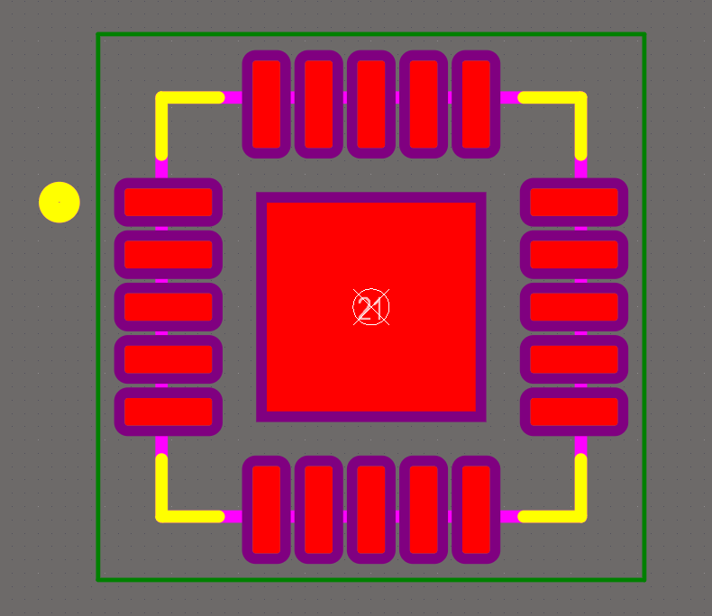
| U1 | ESP32-S3-MINI-1-N8 | SMD Module, ESP32-S3FN8, 8MB SPI Flash | 1 |
| U2 | TL1963A-33DCYR | LDO Regulator 3.3V 1.5A SOT-223 | 1 |
| U3 | FT231XQ-R | IC USB Serial Full UART 20QFN | 1 |
| X1, X2 | M50-1920005 | Shunt Cap Jumper 1.27mm Red | 2 |
Key Components — Symbols, Footprints & 3D
Below I include the schematics, footprints, and 3D views of the three most important components of the project. To ensure visual consistency in the schematic, I redrew the symbols for the MCU, the USB-to-UART converter, and the USB Type-C connector.
ESP32-S3-MINI-1-N8

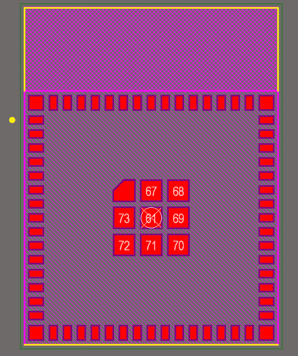

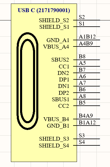
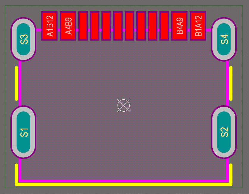
Molex 217179-0001 (USB-C)

FT231XQ-R (USB↔UART)


Schematic Design
Starting from the main blocks, I completed the full schematic: power tree, USB interface, reset/boot logic, crystals, I/O headers and net labeling. Below: overall schematic view.
Linking to PCB & Placement
After pushing from SCH to PCB, components initially appear scattered around the board outline. Through several iterations I organized and placed them to minimize critical lengths and ease routing.
Initial Component Scatter

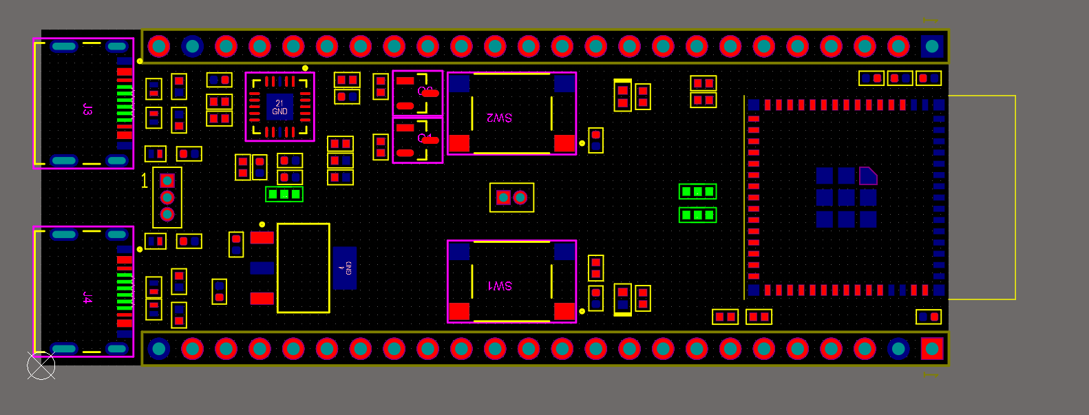
Final Component Placement
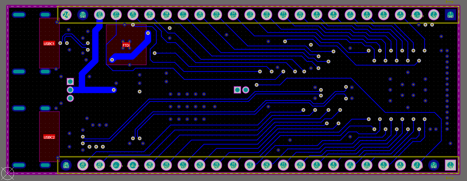
PCB Routing
Routing performed with width rules by current, solid ground planes to reduce noise, and clear layer roles. Below are views for each layer of the 4‑layer stack‑up.
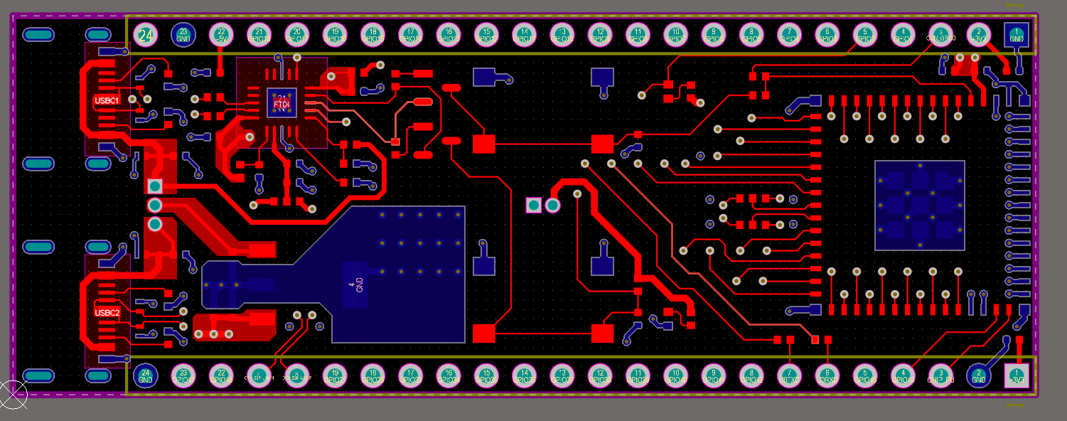
Top Layer (Signal)
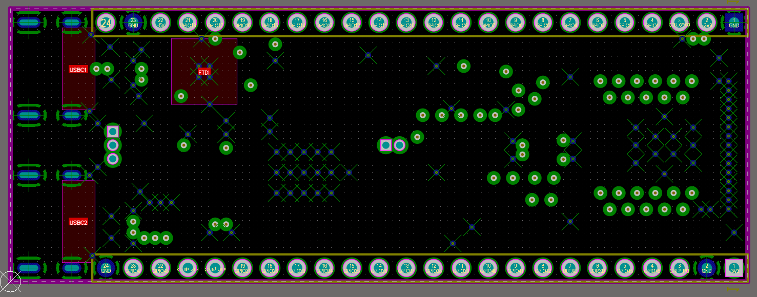
Ground Plane
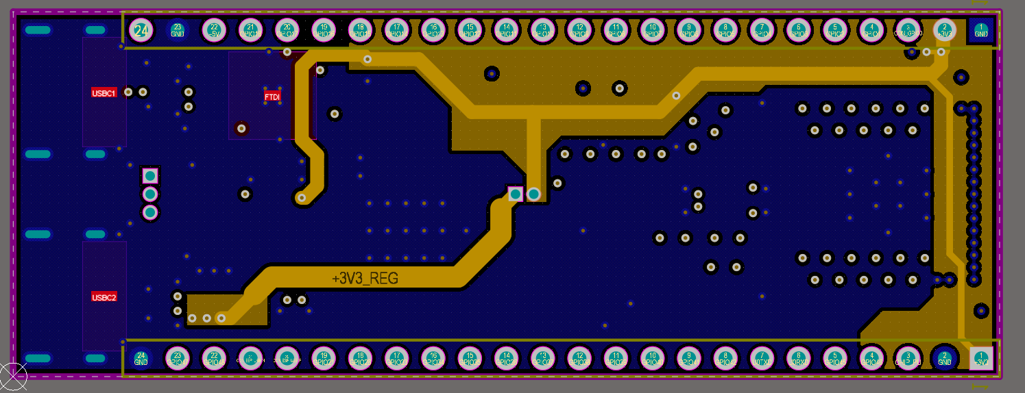
Power Plane
Bottom Layer (Signal)
Final Result
3D renders generated in Altium Designer. Compact layout around the ESP32 module, clear connector access, and readable silkscreen. Ready for fabrication and bring‑up.
Top View

Bottom View

Isometric View
